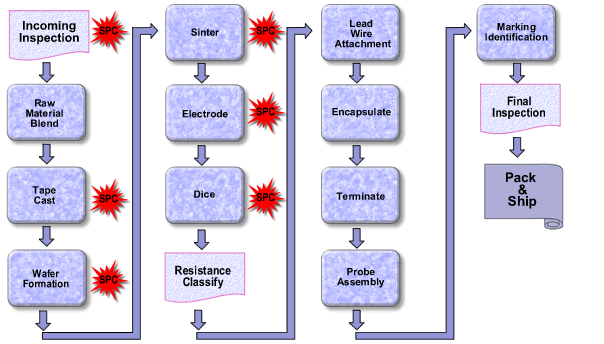
The NTC thermistor manufacturing process can be divided into: Incoming Inspection – Raw Material Blend – Tape Cast – Wafer Formation – Sinter – Electrode – Dice – Resistance Classify – Lead Wire Attachment – Encapsulate – Terminate – Probe Assembly – Marking Identification – Final Inspection – Pack & Ship.
1. Incoming Inspection
All raw materials are inspected upon receipt to verify whether their physical and electrical properties are acceptable. Assign a unique ID# and use it for batch traceability.
2. Raw Material Blend
The manufacture of NTC thermistors begins with the precise mixing of raw materials into organic binder solutions. These raw materials are powdered transition metal oxides such as manganese, nickel, cobalt and copper oxide. Other stabilizers are also added to the mixture. The oxide and binder are combined using a wet process technique called ball milling. In the ball milling process, the materials are mixed and the particle size of the oxide powder is reduced. The finished homogeneous mixture has the consistency of a thick paste. The exact composition of various metal oxides and stabilizers determines the resistance-temperature characteristics and resistivity of the fired ceramic components.
3. Tape Cast
The “slurry” is distributed on a moving plastic carrier sheet using doctor blade technology. The exact material thickness is controlled by adjusting the height of the squeegee above the plastic carrier sheet, the speed of the carrier sheet and by adjusting the slurry viscosity. The casting material is dried on a flat casting belt through a long tunnel oven at high temperature. The resulting “green” tape is malleable and easy to form. Then carry out quality inspection and analysis on the tape. The thermistor tape thickness ranges from 0.001″ to 0.100″ in a wide range, depending on the specific component specifications.
4. Wafer Formation
The tape is ready to be formed into wafers. When thin materials are needed, simply cut the tape into small squares. For thicker wafers, cut the tape into squares and stack it on top of the other. These stacked wafers are then laminated together. This allows us to produce wafers of almost the required thickness. Then, the wafer undergoes additional quality testing to ensure high uniformity and quality. Subsequently, the wafer is subjected to a binder burnout cycle. This method removes most of the organic binder from the wafer. In order to prevent adverse physical stress on the thermistor wafer, precise time/temperature control is maintained during the adhesive burning cycle.
5. Sinter
The wafer is heated to a very high temperature in an oxidizing atmosphere. At these high temperatures, the oxides react with each other and fuse together to form a spinel ceramic matrix. During the sintering process, the material is densified to a predetermined level, and the grain boundaries of the ceramic are allowed to grow. Maintain a precise temperature profile during the sintering process to avoid wafer fracture and ensure the production of finished ceramics that can produce parts with uniform electrical characteristics. After sintering, the quality of the wafer is inspected again, and the electrical and physical characteristics are recorded.
6. Electrode
Ohmic contact with ceramic wafers is obtained using thick film electrode materials. The material is usually silver, palladium silver, gold or platinum, depending on the application. The electrode material consists of a mixture of metal, glass and various solvents, and is applied to the two opposite surfaces of a wafer or chip by screen printing, spraying or brushing. The electrode material is fired on the ceramic in the thick film belt furnace, and the electrical joint and mechanical combination are formed between the ceramic and the electrode. Then check the metallized wafer and record the properties. Precise control in the electrode process ensures that the components produced from wafers will have excellent long-term reliability
7. Dice
High speed semiconductor cutting saw is used to cut the chip into small chips. The saw blade uses a diamond blade and can produce a large number of extremely uniform dies. The resulting thermistor chip can be as small as 0.010 “to 1000”. The chip size difference of a set of chip thermistor chips is actually immeasurable. A typical thermistor chip can produce thousands of thermistor chips. After cutting, clean the chip and check the dimensions and electrical characteristics. Electrical inspections include the determination of nominal resistance values for specific applications, resistance temperature characteristics, production yield, and batch acceptability. Resistance and resistance temperature characteristics are accurately measured within 0.001 ° C using precise temperature control.
8. Resistance Classify
All thermistors are tested for proper resistance values, usually 25 ° C. These chips are usually tested automatically, but they can also be tested manually based on production and specifications. The automatic chip processor is connected to a resistance test device and a computer programmed by the operator to place the chip in various memory areas dependent on its resistance value. Each automatic chip processor can test 9000 parts per hour in a very accurate way.
9. Lead Wire Attachment
In some cases, thermistors are sold in the form of chips and do not require leads, but in most cases leads are required. The thermistor chip is connected to the leads by soldering or by pressure contacts in the diode package. During the welding process, the thermistor chip is loaded on the lead frame, which depends on the spring tension of the wire to maintain the chip during the welding process. The assembly is then immersed in the molten solder pot and removed. The impregnation rate and residence time are precisely controlled to avoid excessive thermal shock to the thermistor. Special fluxes are also used to enhance the solderability without damaging the thermistor chip. The solder adheres to the chip electrodes and leads to provide a firm wire to chip bond. For the diode type “DO-35” package thermistor, the thermistor chip is kept between the two leads in an axial manner. The glass sleeve is placed around the component and heated to high temperature. The glass sleeve melts around the thermistor chip and is sealed to the lead. For example, in a diode structure, the pressure exerted by the glass on the module provides the necessary contact between the lead wire and the thermistor chip.
The leads used for thermistors are usually copper, nickel or alloy, usually tin or solder coating. Low thermal conductivity alloy conductor materials can be used in some applications where thermal isolation between thermistor and conductor is required. In most applications, this allows thermistors to respond to temperature changes more quickly. After attachment, check the bonding between the lead and the chip. A strong welding interface helps to ensure long-term reliability of the completed thermistor.
10. Encapsulate
In order to protect thermistors from operating atmosphere, humidity, chemical attack and contact corrosion, lead thermistors are usually coated with a protective conformal coating. The sealant is usually epoxy resin with high thermal conductivity. Other sealants include silicone, ceramic cement, paint, polyurethane and shrink sleeve. Sealants also help to ensure good mechanical integrity of the equipment. The thermal response of thermistor should be considered when choosing packaging materials. In applications where rapid thermal response is critical, films of high thermal conductivity sealants are used. Where environmental protection is more important, another sealant can be selected. Sealants such as epoxy resin, silica gel, ceramic cement, paint, and polyurethane are usually coated by impregnation and cured at room temperature or placed in an oven at elevated temperatures. Precise time, temperature and viscosity control are used throughout the process to ensure that pinholes or other deformities do not develop.
11. Terminate
Thermistors are usually equipped with terminals connected to the end of their leads. Before the terminal is applied, the insulation on the lead wire is properly stripped to fit the specified terminal. These terminals are connected to the wires using a special tool application machine. The terminals can then be inserted into a plastic or metal enclosure before being delivered to the customer.
12. Probe Assembly
For environmental protection or mechanical purposes, thermistors are usually immersed in the probe case. These enclosures can be made of materials including epoxy, vinyl, stainless steel, aluminum, brass and plastic. In addition to providing suitable mechanical mounting for thermistor elements, the enclosure protects them from the environment they are exposed to. The correct selection of lead, wire insulation and potting materials will result in a satisfactory seal between the thermistor and the external environment.
13. Marking Identification
The finished thermistor can be marked for easy identification. This can be as simple as color dots or more complex, such as date codes and part numbers. In some applications, dyes can be added to the coating on the thermistor body to obtain a specific color. The color dots are usually added to the thermistor by impregnation process. Use a marker to generate tags that require alphanumeric characters. This machine only uses permanent ink to mark parts. The ink solidifies at an elevated temperature.
14. Final Inspection
All completed orders will be inspected for physical and electrical defects on a “zero defect” basis. All parameters are checked and recorded before the product leaves the factory.
15. Pack & Ship All thermistors and components are carefully packaged and will be used by customers.